Invitation - Four-Day EMC Debug Workshop (Biricha)
Thu 14.05.2026
Gain practical skills in solving EMC problems at an intensive 4-day Biricha workshop. This course is based on real hands-on laboratory work.
Four-Day EMC Debug Workshop
by Biricha Digital
Registration here: Four-Day EMC Debug Workshop
Written by Dr Ali Shirsavar in his approachable, easy-to-follow style, this Four-Day EMC troubleshooting and Debugging Workshop is fundamentally different from traditional EMC training. While most EMC courses focus heavily on theory and limited front-of-class demonstrations, in true Biricha style this workshop is built around individual hands-on lab work and real hardware debugging.
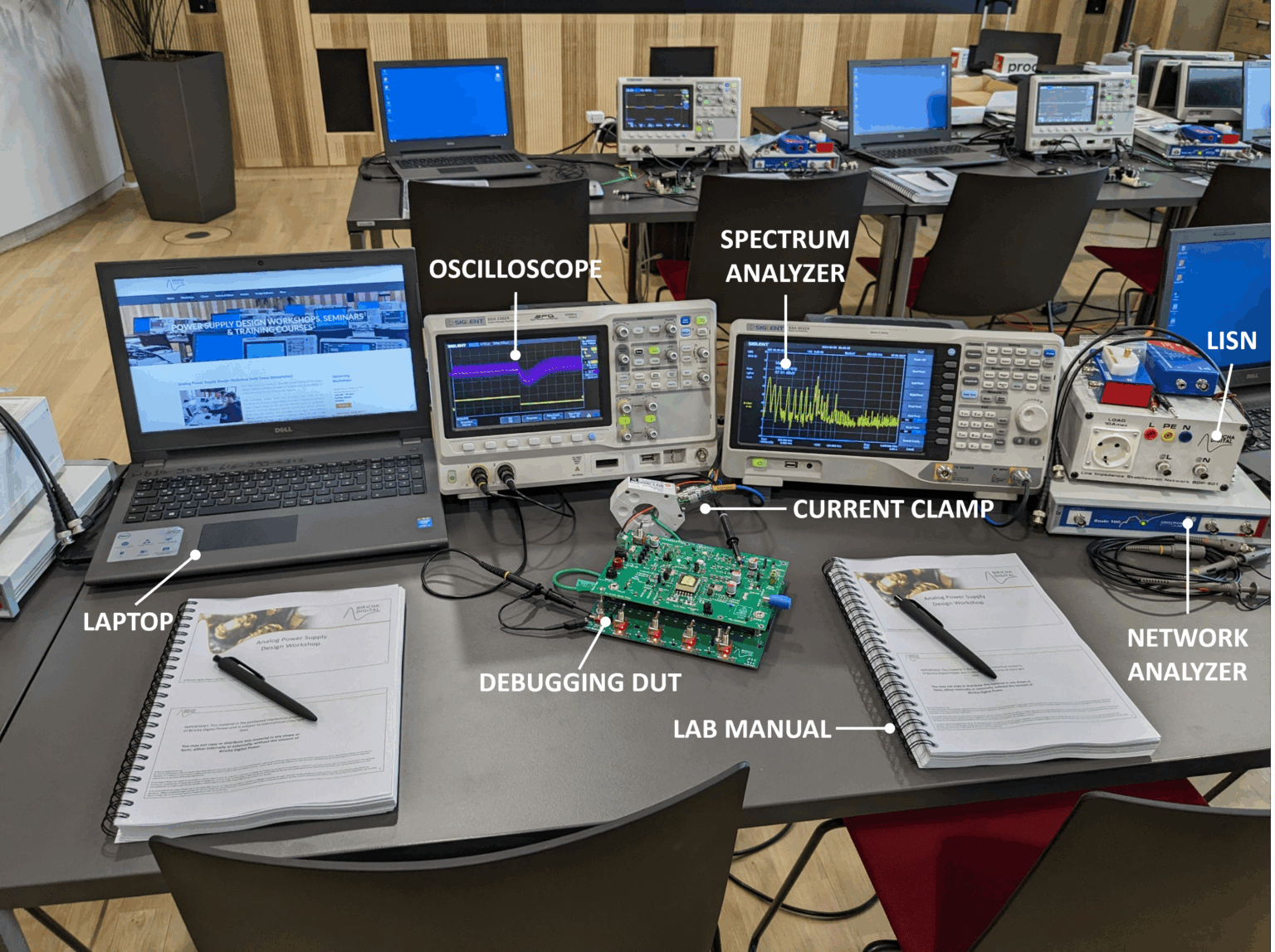
After each theoretical concept is taught, each participant works at their own fully equipped lab station and is provided with specially designed training boards that contain known EMC problems. The students are required to measure, identify, and fix real conducted emissions, radiated emissions, and immunity issues themselves, using professional test equipment including LISNs, spectrum analyzers, network analyzers, current clamps, near field probes, and ESD tools.
The course focuses on hands-on debugging methods that engineers can directly use in real development projects, allowing participants to build repeatable problem-solving skills that can be immediately transferred into their own pre compliance and product development environments..
These workshops are designed for electronic engineers who:
- Need to quickly identify and fix EMC problems during product development
- Want to become confident using EMC measurement equipment for pre compliance debugging
- Are responsible for improving conducted and radiated emissions performance
- Need practical experience with immunity testing and susceptibility troubleshooting
- Want to reduce design iteration cycles and accelerate time to market
- Need structured, hands on EMC training rather than theory only seminars
- Need to add a minimum of 28 hours of continuous professional development hours to their portfolio
Workshop Overview
This Four-Day EMC Debugging Workshop is designed to take engineers step by step from fundamental EMC principles through to practical emissions and immunity debugging. Over four days, participants learn how to identify noise sources, apply effective mitigation techniques, and systematically work toward passing EMC compliance testing.
Starting from EMC fundamentals and measurement techniques, it progressively covers all major EMC debugging domains:
- Conducted emissions debugging (150 kHz to 30 MHz)
- Radiated emissions debugging (30 MHz and beyond)
- Immunity testing and susceptibility fault finding and troubleshooting
- Component selection and mitigation techniques for compliance
Numerous laboratory exercises and debugging examples are based on specially designed training boards that intentionally include common conducted emissions, radiated emissions, and immunity related EMC problems. This allows participants to practice realistic fault finding and mitigation techniques that directly reflect real-world compliance challenges.
Participants work either individually or in pairs at one of 10 fully equipped EMC debugging workstations. Each station includes a pre-compliance LISN, spectrum analyzer, current clamp, near-field probes, ESD equipment, and supporting laboratory instrumentation required for emissions and immunity debugging. This setup ensures that every attendee actively performs measurements, debugging, and mitigation verification throughout the course.
To maintain a high level of hands-on participation and instructor interaction, the total number of attendees is strictly limited to 20 per engineers session. This guarantees sufficient lab equipment, direct instructor support, and meaningful individual practice time.
Upon successful completion of the workshop, participants receive a certificate for their professional development records. Attendance and active participation throughout the majority of the workshop sessions are required to qualify for certification.
Agenda (total 28 hours of CPD)*
Day 1: EMC Fundamentals and Debugging Foundations
- Fundamentals of EMC compliance and testing concepts
- Understanding conducted and radiated emissions measurement principles
- Noise coupling mechanisms including capacitive, inductive, and electromagnetic field coupling
- Linking frequency-domain noise signatures to real circuit boards and layout coupling paths
- Step-by-step EMC debugging workflow
- Hands-on labs include:
- Hands-on operation of LISNs, spectrum analyzers, current clamps, near-field probes, and ESD tools
- EMC instrument setup and pre-compliance measurement techniques
- Noise coupling demonstrations and reflection experiments
- Frequency-domain noise pattern recognition exercises on real hardware
Day 2: Conducted Emissions Debugging and Mitigation (150 kHz to 30 MHz)
- Fundamentals of conducted emissions measurements and regulatory limits
- Identifying dv/dt-related capacitive noise mechanisms
- Identifying di/dt-related magnetic coupling mechanisms
- Ringing and resonance identification in switching power supplies
- EMC input filter fundamentals and compliance-driven filter design concepts
- Hands-on labs include:
- Real conducted emissions debugging in our lab including:
- LISN-based noise observation and root cause identification
- Debugging techniques and EMC fault finding using a spectrum analyzer and a LISN
- Snubber tuning and switching noise mitigation demonstrations
- EMC input filter performance verification
Day 3: Radiated Emissions Debugging and Mitigation (30 MHz and Beyond)
- Understanding radiated emissions testing and how they relate to bench measurements
- How to use current clamps to locate radiation failure sources on cables and PCBs
- PCB-level noise source localization using near-field probes
- High-speed digital and clock-related radiation mechanisms
- Hands-on labs include:
- Current clamp-based cable and PCB radiation analysis
- Near-field probe PCB scanning and hot-spot identification
- High-speed clock and digital noise fault finding exercises
- Debugging circuits with multiple clocks and switching frequencies
Day 4: EMC Immunity Testing and Susceptibility Debugging
- Radiated and conducted immunity test fundamentals and performance criteria
- Understanding EFT, surge, and ESD disturbance mechanisms and real-world interference sources
- Debugging using ESD stress testing to locate susceptibility points and weak design areas
- MOV/TVS and Clamp-on ferrite core selection techniques for immunity improvement
- Hands-on labs include:
- Locating and fixing susceptibility issues using controlled ESD stress testing
- Noise injection techniques using current clamps for susceptibility testing
- Using EMC input filters to improve conducted immunity susceptibility performance
- Comparing poor versus optimized PCB layouts to evaluate layout impact on immunity behavior
Place of the workshop in Europe
Monday 30th November - Thursday 3rd December 2026
Freiham, Munich, Germany
Workshop Language is English
2950 EUR for 4 days